Packaging Information

This section is intended to give you access to up-to-date CML Micro (encapsulation) package information. CML Micro publications containing specifications of all CML Package Styles, Tape and Reel Dimensions and Solder. Package information specific to each product is provided on our Product pages, in the ‘Package’ tab at the bottom of each page.

Tape and Reel Specification

QFN PCB Design Guidance Notes

Packaging Despatch

Solder Reflow Profiles

Note: For the purposes of this page, the physical IC connection descriptions of ‘pin’, ‘leadless’ and ‘pin’ etc. are represented by the single term of ‘pin’.

VQFN Packages FAQs

Q. What recommendations can CML provide to me when considering the use of the VQFN (Very Thin Quad Flat Non-leaded) package and what is the best way to attach a CML device supplied in this package to my PCB?

A. CML supplies a number of devices in VQFN packaging. Due to their compact size, the devices available in these package types are called “Qx” packages, where x is a reference to the number of pins available (e.g. Q1 = 64 pins).


CML advises that special care should be taken when assembling any Qx (e.g. Q1 64 pin VQFN) packages on to a PCB.
In some cases, such as the CMX990 and the CMX998, it is necessary for both electrical and thermal dissipation reasons to attach the central exposed pad to a ground plane on the PCB.


In other cases, unless stated to the contrary, it is not essential for electrical or thermal dissipation reasons to make such connection, however CML would still recommend that this pad be soldered down to the PCB so as to provide good physical attachment. If this is done, the PCB land to which it is attached should be electrically unconnected to other parts of the PCB.

The following link will take the reader to a CML guidance note on using the CML VQFN package. It provides comprehensive guidance for assembling such packages into an application QFN PCB Design Guidance Notes.

Q. I am a user of a CML part that is supplied in a QFN package. Will all supplied packages be identical and is there any possible variation I should be aware of which should be considered when laying out my PCB?

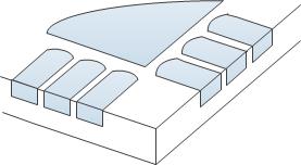
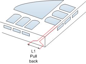
A. CML Microcircuits may supply two subtly different QFN/WQFN packages as stated in the datasheet.


QFN/WQFN with no Pull-back


QFN/WQFN with Pull-back


With regard to mounting this package (reference to IPC610) solder toe fillets are not required or achievable on the side walls of all QFN/WQFN Packages.


Cross-Section View of an Acceptable Solder Joint on QFN/WQFN Packages with Pull-back Design

Latest News

CML launches sub-GHz band GaAs 2W linear power amplifier to ease UHF system development

24 September 2024
Maldon, Essex, UK – CML Micro extends its SµRF range of sub-GHz MMICs with a 2 W power amplifier optimized for linear performance and...

Latest News

CML launches the CMX90A705 Ka-band GaN power amplifier for cost-effective development of commercial satcom terminals

18 June 2024
Maldon, Essex, UK – CML Micro has announced the launch of a Ka-band gallium nitride (GaN) power amplifier that represents a cost-effective...

Latest News

DRM1000 - The world's most versatile DRM Receiver

20 May 2024
Maldon, Essex - 19 May 2024 - CML Micro has today announced the global availability of the DRM1000 module - a complete Digital Radio Mondiale...

Latest News

Executive Interview with Microwave Journal

20 February 2024
An executive interview with Mark McCabe, Managing Director and Ion Furtuna, Senior VP of Sales at CML Micro with Microwave Journal. 1. Can you...
Register here for newsletter and product launch notifications
By submitting this form, you agree to subscribe to our mailing list and receive updates from us. Please see our privacy policy.