Wireless Data
CMX589A – Versatile Full-duplex GMSK Modem
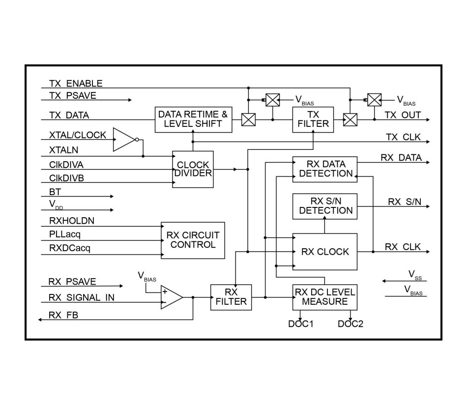
The CMX589A is a single-chip full-duplex synchronous data GMSK modem designed for Wireless Data Applications. Employing Gaussian filtering for Minimum Shift Keying baseband modulation applications, the CMX589A features a wide range of available data rates from 4000 to 200000 (200k) b/s
Data Rates and the choice of BT (0.3 or 0.5) are pin programmable to provide for different system requirements.
The Tx and Rx digital data interfaces are bit serial, synchronized to generated Tx and Rx data clocks. Separate Tx and Rx Powersave inputs allow full or half-duplex operation. Acquisition, Lock, and Hold of Rx data signals are made easier and faster by the use of Rx Control Inputs to clamp, detect, and/or hold input data levels and can be set by the µProcessor as required.
Devices are available through our Distributor Network.
Features
- Full Duplex (GMSK)
- Data Rates: 4kbps to 200kbps
- Selectable BT: 0.3 or 0.5
- Low Current Non-DSP Solution
Applications
- Meets RCR STD-18
- Wireless LAN/Modems
- Rx Only AIS Monitors
- Automatic Vehicle Location Links
- Wireless Data Links for PCs, Laptops and Printers
- Point-Of-Sale Terminals
- Wireless Bar-Code Readers and Stock Controllers
- Wireless Local Loop
- Amateur Packet Radio
- Wireless ISDN
Power Supply Requirement
- 3.0 to 5.5 V
Downloads
Design Resources
FX589 and CMX589A FAQ
Q. What tone frequencies are on the output of a GMSK modem?
A. Tone frequencies are not used to carry data in GMSK. GMSK = Gaussian Minimum Shift Keying – The data is shaped through a Gaussian filter and then directly modulated onto an FM radio carrier.
Q. The BER (Bit Error Rate) is high, what I am doing wrong? A. There are a number of documents available to describe reliable operation of these devices:
- FX589 GMSK Modem application note: app589_2 describes the modulation scheme and typical problems that occur. This also explores AC and DC coupling issues.
- Increasing Data Throughput in Radio Telemetry Systems. The application note: app589_2 describes gaussian filtering and various schemes to reduce bit errors and, should they occur, how to detect and correct them.
Buffering circuits for the CMX589A input and output can be found in the schematic for the EV9000 Evaluation Kit in the Obsolete Products Archive. Use the link in the left hand pane to navigate to the Archive. Scroll down to the EV9000 and click on the link Support File. Also remember that very low level signals will be seen at minimum sensitivity so good layout practice should be followed both on production PCBs and when evaluating.
Q. 589 What is the difference between the FX589 and the CMX589A? A. There is virtually no difference between these devices as the CMX589A was made pin and function compatible with the FX589. Customers are advised to switch to the CMX589A although CML will continue to support users of the FX589.
Q. Can I change the transmit BT to 0.4? A. Yes. R1 and C1 form the final pole of the transmit filter and determine the rolloff characteristic of the ‘589. Changing the filter values will change the BT but this is dependent on the data rate. If a BT of 0.5 is selected then at a data rate of 9600 bps, C1 should be changed to 680pF. C1 will scale for other data rates.
Q. How do I view the “eye diagrams” for the CMX589A? A. A two-channel oscilloscope is needed for this testing. In general, one channel of the oscilloscope should be placed on the signal path of interest, such as the Tx output (after the external RC filter) or Rx input. The other oscilloscope channel should be used for triggering and should ideally be placed on the transmitting CMX589A “Tx CLK” signal. This will allow the triggering to be synchronized with the completion of each transmitted data bit. If this triggering location is not practical, use the receiving CMX589A “Rx CLK” signal for triggering. Either edge of the Tx/Rx CLK signal can be used for triggering. The data stream used for this testing should have a reasonably random structure.
Q. The DC level of the Tx Output pin is shifting excessively when I switch the state of the Tx Enable pin. Why is this happening? A. The CMX589A Tx Output pin DC level doesn’t shift appreciably unless the pin is being loaded. This loading can be caused either by test equipment probes or connected devices. When the Tx section is not powersaved, the Tx Output pin can be in one of two states; enabled and disabled. In the disabled condition, the Tx Output pin is connected to Vbias through a 500kohm internal resistance. Any loading on the Tx Output pin, including “10x” oscilloscope probes, dirty solder connections, or connected devices with low input impedance, will create a voltage divider effect and can cause the DC level on the Tx Output pin to decrease. To prevent any loading of the Tx Output pin, all connections to the Tx Output pin should have very high input impedance. A buffer amplifier is a good way to prevent loading of the Tx Output pin.
Two-point modulation Theory
Using two-point modulation to reduce synthesiser problems
CDPD Solutions
Cellular Digital Packet Data (CDPD)
Practical GMSK data transmission
Practical GMSK data transmission

