Wireless Data
CMX469A -1200/2400/4800 Baud FFSK Modem
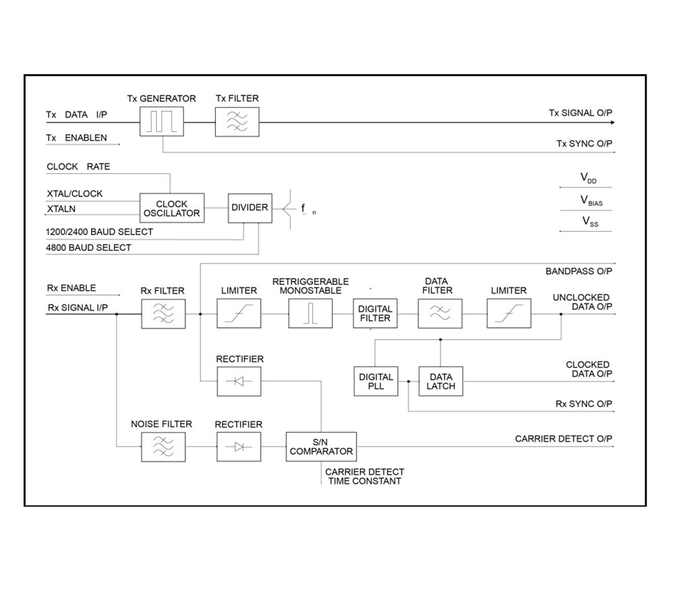
The CMX469A is a CMOS LSI circuit which operates as a full-duplex 1200, 2400 or 4800 baud FFSK Modem.
The mark and space frequencies are 1200/1800, 1200/2400 and 2400/4800Hz respectively. Tone frequencies are phase continuous; transitions occur at the zero crossing point.
A common Xtal oscillator is employed with a choice of two clock frequencies (1.008MHz or 4.032MHz) to provide baud-rate, transmit frequencies, and Rx and Tx synchronisation.
The modem includes circuitry for Carrier Detect and Rx Clock recovery, both of which are made available as output pins. Rx, Tx and Carrier Detect paths contain a bandpass filter to ensure the provision of optimum signal conditions.
The CMX469A demonstrates a high sensitivity and good bit-error-rate under adverse signal conditions.
This low-power device requires few external components and is available in small outline plastic SOIC and TSSOP packages.
Devices are available through our Distributor Network.
Features
- Selectable Data Rates: 1200/2400/4800 Baud
- Full Duplex FFSK
- Rx and Tx Bandpass Filters
- Clock Recovery and Carrier Detect Facilities
- Pin Selectable Xtal/Clock Inputs:
– 1.008MHz or 4.032MHz - Simple Control: No µP Required
Applications
- Data-Over-Radio
- PMR and Cellular Radio Signalling
- Automatic Vehicle Location (Differential GPS) Links
- Portable Data Terminals
- Personal/Cordless Telephone
- Industrial Control Signalling
Power Supply Requirement
- 2.7 to 5.5 V
Downloads
Design Resources
CMX469A - Simple Data Communications
Simple Data Communications with the CMX469A
CMX469A Firmware
Firmware listing (text file) for the above CMX469A Application Note
MX469 to CMX469A
Design Migration from MX469 to CMX469A
FX/CMX469A FAQ
Q. I currently have a 10kohm pullup resistor on each of the RX SYNC and CARRIER DETECT O/P pins. Will this cause a problem?
A. Yes it will. The digital output impedance of those pins is typically 4000 ohms. When a 10kohm pullup resistor is attached to each of those pins, a voltage divider is created that prevents the voltage on those pins from approaching the expected “low” value of near 0V. This can cause problems for a microcontroller that is monitoring the signal on those pins. For example, the higher-than-expected voltage on the CMX469A digital output pin (with an attached pullup resistor) may not reach the microcontroller’s digital low “threshold” value, and this can cause lots of problems.
Q. What is the difference between the FX469 and the CMX469A?
A. There are no major differences between the FX469 and the CMX469A. The CMX469A is the preferred device for new designs and it posesses the advantage of operation down to 2.7V DC. For those customers contemplating migration to the CMX469A there is a difference in the operation of the Carrier Detect Output that may be important. When powersaved the FX469 Carrier Detect always returns to Vss (low).
The CMX469A however, always maintains its last state.
Thus a CMX469A that is powersaved while receiving FSK data will maintain its Carrier Detect high.
Current consumption is the same, 4.5mA at 5V, but this can be further reduced at 3V to 2mA, giving significantly reduced power consumption.
The CMX469A is also available in a smaller package: A TSSOP for space constrained designs.
Q. Why does the CMX469A generate interrupts for received data when there is no data present?
A. The FFSK receiver of the CMX469A has a very high sensitivity and in the absence of valid signals will decode noise as data. This is not a fault but is due to the wideband properties of noise where sufficient energy may be present within the FFSK decoder’s bandwidth. To prevent spurious reception a baseband carrier detect output (CARRIER DETECT O/P) is used to determine the validity of the received signal.
The detector block comprises a comparator fed from two sources, one sourcing predominantly in-band (FFSK) energy through the decoders band-pass filter and the other sourcing wideband energy through a wider band-pass (noise) filter. The two levels are continuously compared so that when the in-band energy is significantly above the background noise energy, the CARRIER DETECT O/P is set high.
To qualify the presence of FFSK, the CARRIER DETECT O/P is not set high immediately. The comparator output triggers a re-triggerable monostable whose time constant is determined by an external RC pair. The time constant can be varied to give the optimum trade-off between response time and immunity to false indication. The CARRIER DETECT O/P should be monitored during reception and used to ‘intelligently’ decide whether the data is likely to valid, suspect or invalid. During periods when there is no data reception the CARRIER DETECT O/P will be predominantly low but is likely to false so the receiver should be powersaved where practical.
The CARRIER DETECT O/P does not internally gate the FSK receiver because this would prevent data reception during short duration events such as fades when data recovery may still be possible.
Q. Does it matter which edge of the “Tx Sync” signal I use to strobe Tx data in on?
A. Yes it does. The rising edge of the Tx Sync (data clock) signal determines when the data is latched into the CMX469A. The data must be valid for 2.0us before and after the rising edge; otherwise erroneous operation will result.

